NVIDIA has invested $3.5 billion in MediaTek convertible bonds, alongside an expanded partnership announced on August 31, 2026. For data-centre customers, the central development is MediaTek's planned use of NVLink Fusion to help build custom AI accelerators for NVIDIA-connected racks. The agreement also covers future RTX Spark and DGX Spark PC chips and automotive platforms. Company announcement.
What MediaTek will offer
Customers will be able to bring accelerator designs to MediaTek and customize connectivity, memory, packaging, power and performance. NVIDIA and MediaTek say they will supply the surrounding engineering and manufacturing support needed to take those designs toward rack-scale deployment.
The release does not name a customer for this particular custom-XPU program, identify a finished accelerator or give its delivery date. It also leaves out the bond conversion price and maturity. The confirmed investment amount should therefore be kept separate from estimates of a future ownership percentage. NVIDIA–MediaTek release.
Three technologies with different jobs
NVIDIA's NVLink Fusion platform documentation describes the surrounding components:
| Technology | Role around a custom accelerator |
|---|---|
| NVLink Fusion chiplet and scale-up fabric | Connect accelerators into a shared rack-scale compute domain. |
| NVLink-C2C | Provide a coherent chip-to-chip connection between custom silicon and compatible NVIDIA processors. |
| NVHBM | Combine a custom HBM base die and NVIDIA-designed memory controller to change how memory connects to the compute die. |
The platform page specifies 260 TB/s across a 72-accelerator NVLink 6 domain. That is an aggregate fabric figure; it is not a per-chip C2C speed or a specification for an announced MediaTek product. Keeping those scopes separate matters when comparing system diagrams or procurement proposals.
Why the memory design matters
NVIDIA's NVHBM technical explanation describes moving the memory controller into the HBM stack and using a custom physical interface. The intended benefit is more room for compute and less overhead moving data into it.
NVIDIA reports up to 30% more memory bandwidth and up to 15% lower HBM power consumption than standard HBM4e. Those are vendor comparisons for the memory technology, not independently measured results for a MediaTek accelerator. A percentage reduction in memory power also cannot be applied to an entire rack's electricity bill: processors, networking and other systems contribute to that total.
What to watch before calling this deployed capacity
Our assessment: the partnership's significance is the engineering route it offers. A customer can pursue a specialized compute design while retaining NVIDIA technology around it. Whether that approach improves delivery time or economics will depend on the actual product and workload.
The useful next disclosures would be a named customer, a qualified package, a delivery schedule and workload-specific measurements. For operators, the practical questions include the rack's power envelope, cooling requirements and software support. A financing announcement alone cannot answer those questions or establish how much new compute is operating.
For the facilities context, see our GB300 power and cooling explainer and NVIDIA 800 VDC rollout guide.
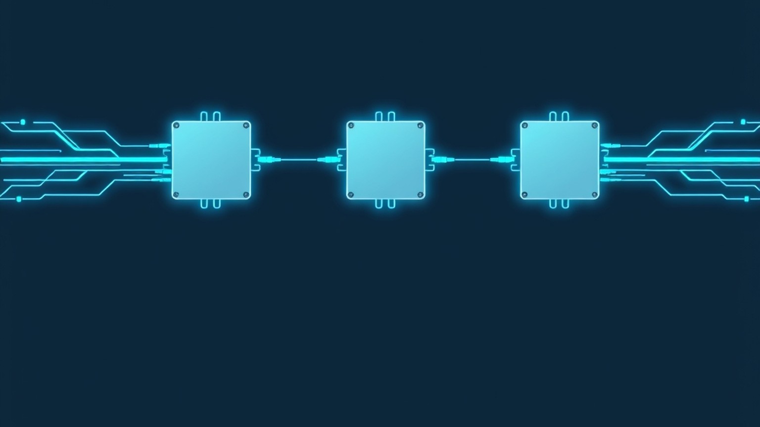
Cover: AI-generated conceptual illustration of connected processors; not a product photograph.
Sources
This article was researched and fact-checked against the following sources:
- Nvidia Bets $3.5B on MediaTek Convertible Bonds, Fueling Circular Financing Debate (techtimes.com)
- NVIDIA MediaTek Partnership Deepens With $3.5 Billion Investment, NVLink Fusion XPUs, and RTX Spark PCs - StorageReview.com (storagereview.com)
- Nvidia commits $3.5 billion to MediaTek bond deal as custom AI-chip strategy expands | MLQ News (mlq.ai)
- Your privacy choices (finance.yahoo.com)
- NVIDIA Invests $3.5B in MediaTek, Expands AI Alliance (cloudnews.tech)
- NVIDIA and MediaTek expand their partnership — company announcement (nvidianews.nvidia.com)
- NVIDIA NVLink Fusion platform documentation (www.nvidia.com)
- NVIDIA NVLink Fusion Brings NVHBM to Next-Generation AI Infrastructure (developer.nvidia.com)